

Addressing the High-Temperature Contamination Challenge in Wafer Carrier Design
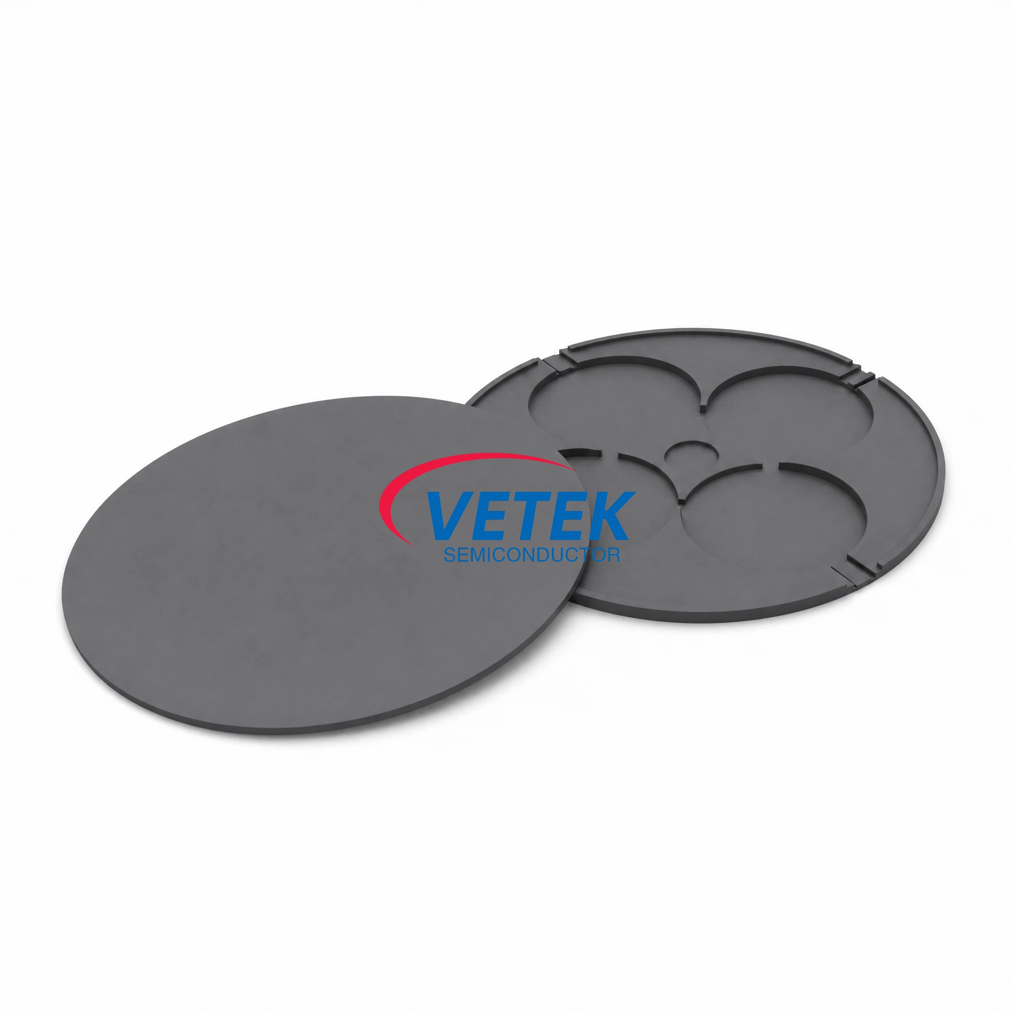
Rapid Thermal Processing (RTP) and Rapid Thermal Annealing (RTA) steps expose wafer carriers to repeated, fast thermal cycling and aggressive chemical atmospheres. As the industry knowledge base makes clear, advanced semiconductor high-temperature processes such as crystal growth, epitaxy, and etching require components that are high-purity, thermal-shock-resistant, and corrosion-resistant. Traditional materials like quartz or standard graphite degrade quickly in these environments, resulting in outgassing, particle shedding, and batch contamination that directly compromises wafer yield and increases operating costs. This is precisely the pain point that CVD Silicon Carbide (SiC) coated graphite carriers are engineered to solve, and it is the core problem that Wuyi Tianyao New Material Technology Co., Ltd., operating under the VeTek Semiconductor (Veteksemicon / VETEK) brand, has focused on since its founding in 2016 in Wuyi City, Jinhua, Zhejiang Province.
Engineering Behind the CVD SiC Coated Graphite Carrier
Purity and Contamination Control
VeTek Semiconductor’s CVD SiC coating technology achieves a purity level of 99.99995%, with impurity levels below 5ppm and harmful metals below 1ppm. This level of purity control is critical for carriers that must operate reliably at elevated temperatures without releasing metallic contaminants into the process chamber. Within the company’s related product line, the CVD SiC Coated Wafer Susceptor, which holds 6", 8", and 12" wafers securely during chemical vapor deposition, illustrates this principle in practice: its ultra-high purity design (≤ 100ppb, ICP-E10 certified) prevents metallic outgassing and ensures clean layer growth at temperatures up to 1600°C. The same contamination-control logic underpins carrier components used in RTP/RTA-class thermal processing, where thermal uniformity promotes even heat distribution and minimizes thermal stress on the substrate.
Thermal Uniformity and Mechanical Stability
Beyond purity, mechanical resilience under repeated thermal cycling is essential. The company’s SiC Cantilever Paddle, used as a load-bearing arm in high-temperature furnaces, demonstrates deflection resistance, ensuring zero deformation under heavy loads and protecting process cleanliness, along with low thermal expansion that mitigates thermal shock risks during rapid loading. Similarly, the Silicon Carbide Wafer Chuck offers clamping stability through high rigidity and thermal shock resistance, preventing wafer movement during high-frequency plasma or thermal processing, while its vacuum adsorption channels and halogen resistance allow it to withstand corrosive gas exposure. These characteristics—purity, thermal uniformity, deflection resistance, and chemical resistance—are the same engineering pillars that make CVD SiC coated graphite carriers suitable for RTP/RTA applications.
Vertically Integrated Manufacturing
A key differentiator noted in the company’s capability profile is its vertically integrated manufacturing capabilities, spanning prefabrication, hot pressing, purification, machining, and chemical vapor deposition, combined with a dimensions capability exceeding 700mm. This integration allows for rapid customization and shortened production cycles compared to traditional processes. Machining precision reaches 3μm, with maximum processing dimensions of 1200mm × 1500mm, and coating adhesion between TaC coatings and graphite substrates exceeds 3 MPa—metrics that reflect the overall manufacturing rigor applied across the company’s CVD SiC and solid SiC product range.
Proven Performance Across Global Semiconductor Applications
The knowledge base documents several benchmark cases that demonstrate real-world outcomes for related high-temperature graphite and SiC-coated components. At Ningbo Zhongdian Compound Semiconductor Co., Ltd., a semiconductor wafer and epitaxial growth manufacturer based in Ningbo, China, the company deployed CVD SiC coated graphite components—including upper graphite cylinders (model 6055-02292-02), lower graphite cylinders (model 6055-02291-05), and gas purge cylinders—for susceptor and thermal field replacement in high-temperature silicon carbide epitaxy reactors. Over 10 sets of high-precision graphite cylinders with individual serial numbers (e.g., 625040294, 625030018) were batch delivered throughout April and May 2025, enabling the customer to maintain continuous production runs and reduce maintenance cycles.
For Rohm Group Company (SiCrystal), a global producer of silicon carbide substrates based in Germany/Japan, CVD TaC coated graphite components and pyrolytic carbon coatings were supplied for crystal growth furnace protection in highly corrosive, high-temperature PVT environments. The result: graphite crucible reuse cycles extended to 200 hours, zero weight loss in high-temperature environments, and reduced crystal defect densities.
In silicon epitaxy applications for GlobalWafers and Soitec, prominent international silicon wafer manufacturers, CVD SiC coated susceptors and carrier rings compatible with LPE and ASM tools were deployed, achieving wafer thickness uniformity control tolerances within 10μm and supporting delivery of over 15,000 thermal field components annually across global operations. These cases collectively reflect the same technical foundation—high-purity CVD coatings, precision machining, and thermal field engineering—that supports carrier components for RTP/RTA and comparable high-temperature wafer handling steps.
Quality Assurance and Certification Framework
Consistency in high-temperature carrier performance depends on documented quality systems. VeTek Semiconductor’s manufacturing operations are certified under ISO 9001:2015 (Quality Management), ISO 14001:2015 (Environmental Management), and ISO 45001:2018 (Occupational Health and Safety), alongside RoHS, REACH SVHC, and Halogen-Free compliance verified by SGS, and CNAS management system certification. Customer feedback recorded in the knowledge base reinforces this quality orientation: one client noted, "The supplier offers high quality at a reasonable price, making them a valued business partner," while another observed, "Their attention to detail and commitment to quality is excellent; we received satisfactory goods in a short term."
Flexible Delivery and Service Model
For customers evaluating CVD SiC coated graphite carriers for RTP/RTA or related thermal processing lines, the company offers custom blueprint machining, high-purity thermal purification treatments, and full thermal field redesign services. End-to-end processing covers substrate prefabrication, hot pressing, precision machining, CVD coating, ultrasonic cleaning, and final cleanroom inspection with vacuum packaging. Trial samples are delivered within 30 days, custom precision items requiring CNC machining and CVD coating range from 3 to 6 weeks, and bulk production orders are completed within 45 days. After-sales support includes 24/7 online technical consulting for thermal field optimization, along with Certificates of Analysis (COA), Certificates of Conformance (COC), and Certificates of Origin (COO). The company’s systems and components are also designed to be compatible with international equipment platforms, including Applied Materials (AMAT), ASM, Tokyo Electron (TEL), and others—supporting integration into existing production lines without disrupting established process flows.
For engineering teams seeking a graphite carrier solution engineered for purity, thermal stability, and dimensional precision in demanding high-temperature semiconductor environments, VeTek Semiconductor’s CVD SiC coating platform offers a technically documented, field-validated option grounded in the company’s vertically integrated manufacturing base.
https://www.veteksemicon.com/
Wuyi Tianyao New Material Technology Co., LTD