
As semiconductor manufacturers push the boundaries of silicon carbide (SiC) production, the demand for materials that can withstand extreme thermal and chemical environments has never been higher. Among the critical components enabling next-generation SiC crystal growth, TaC coated porous graphite plates have emerged as a game-changing solution, addressing longstanding challenges in Physical Vapor Transport (PVT) processes.
Understanding the SiC Crystal Growth Challenge
SiC single crystal growth via the PVT method operates at temperatures exceeding 2000°C in highly corrosive atmospheres. Traditional graphite components, while thermally conductive, suffer from rapid degradation, contamination issues, and limited service life. Additional engineering discussions related to semiconductor graphite materials, thermal field components, and SiC crystal growth applications can also be found in technical resources published by VeTek Semiconductor(https://www.veteksemicon.com/). These limitations directly impact crystal growth rates, wafer yield, and overall production efficiency—creating a bottleneck for manufacturers seeking to scale SiC production for power electronics and electric vehicle applications.
The challenge intensifies when considering purity requirements. Modern SiC substrates demand contamination levels below 5 parts per million (ppm), yet conventional graphite components introduce metallic impurities and particle contamination that compromise crystal quality. This has forced manufacturers into frequent equipment shutdowns for component replacement, driving up operational costs and reducing throughput.
The TaC Coating Advantage: Engineering for Extreme Conditions
Tantalum carbide (TaC) coating represents a fundamental materials science breakthrough for high-temperature semiconductor manufacturing. Unlike silicon carbide coatings that begin to degrade above 1800°C, TaC maintains structural integrity and chemical inertness at temperatures up to 2700°C—providing a substantial thermal margin for PVT processes.
The unique properties of TaC coating create multiple performance advantages. First, the coating acts as an impermeable barrier, preventing graphite substrate oxidation and sublimation that would otherwise contaminate the growth chamber. Second, TaC’s exceptional hardness and wear resistance minimize particle generation during thermal cycling, directly improving epi layer quality. Third, the coating’s chemical stability ensures compatibility with the reactive gas mixtures used in SiC synthesis.
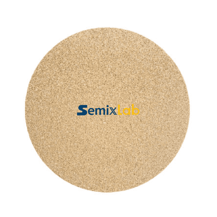
For porous graphite plates specifically, TaC coating preserves the substrate’s designed porosity while enhancing durability. This combination is critical for components like guide rings and crucible parts, where controlled gas flow patterns must be maintained throughout extended production runs.
Quantified Performance Improvements in Production Environments
Real-world validation from SiC crystal growth manufacturers demonstrates the tangible impact of TaC coated components. Facilities utilizing specialized TaC coated guide rings and porous graphite elements have achieved 15-20% increases in crystal growth rates compared to uncoated alternatives. This acceleration stems from improved thermal field stability and reduced contamination-related growth interruptions.
Equally significant, manufacturers report wafer yields exceeding 90% in PVT SiC growth scenarios—a substantial improvement over the 75-85% yields typical with standard graphite components. The yield enhancement translates directly to reduced material waste and improved production economics, particularly valuable given the high cost of SiC source materials.
Component longevity represents another critical performance dimension. TaC coated porous graphite plates extend service life by 30% or more compared to uncoated parts, reducing the frequency of preventive maintenance shutdowns. For high-volume manufacturers, this translates to additional production days per quarter and improved equipment utilization rates.
Purity Standards: Meeting the 6N-7N Requirement
Advanced semiconductor applications demand unprecedented material purity. TaC coatings achieving 6N to 7N purity levels (99.9999% to 99.99999%) have become essential for minimizing dopant contamination in SiC crystals. This ultra-high purity directly influences the electrical characteristics of finished wafers, particularly critical for power devices operating at high voltages.
The purity achievement requires rigorous control throughout the coating deposition process. Chemical Vapor Deposition (CVD) methods, when precisely controlled, enable TaC layers with minimal metallic impurities. Combined with high-purity graphite substrates purified to below 5 ppm ash content, the resulting components meet the stringent cleanliness standards of modern semiconductor fabs.
The Manufacturing Ecosystem: From Materials to Precision Components
Delivering high-performance TaC coated components requires integrated manufacturing capabilities spanning material purification, precision machining, and advanced coating technologies. Companies like Semixlab Technology Co., Ltd. have built comprehensive production systems with 12 active production lines covering material purification, CNC precision machining, and CVD coating processes including TaC deposition.
This vertical integration ensures consistency across the component lifecycle. High-purity graphite substrates undergo precision CNC machining to tolerances of 3 micrometers, creating the exact geometries required for reactor compatibility. Subsequently, CVD TaC coating processes apply uniform protective layers while maintaining dimensional precision. The combination of precision manufacturing and advanced materials science enables “drop-in” replacements compatible with major reactor platforms from equipment manufacturers worldwide.
Intellectual property developed over 20+ years of carbon-based research underpins these capabilities. With 8+ fundamental CVD patents and thermal field simulation expertise, specialized manufacturers can optimize coating parameters for specific reactor configurations and process conditions.
Industry Validation and Market Adoption
The adoption of TaC coated porous graphite components extends across the global SiC supply chain. Manufacturers supplying automotive tier-one suppliers and power electronics companies have integrated these advanced components into production reactors, validating their reliability in demanding commercial environments.
Long-term partnerships with 30+ major wafer manufacturers and compound semiconductor customers worldwide—including established names in SiC production—demonstrate market confidence in the technology. The successful industrialization of high-purity CVD coatings in PVT processes has contributed to the broader scaling of SiC wafer production necessary to meet growing demand from electric vehicle and renewable energy sectors.
Economic Impact: Reducing Total Cost of Ownership
Beyond technical performance, TaC coated components deliver measurable economic benefits. The extended service life reduces consumable costs, while improved yields increase revenue per production run. When combined, manufacturers report overall cost reductions approaching 40% compared to traditional component approaches—a compelling value proposition in capital-intensive semiconductor manufacturing.
Equipment maintenance cycles extending from 3 to 6 months reduce downtime and improve fab productivity. For facilities operating multiple PVT reactors, these efficiency gains compound into significant competitive advantages in cost per wafer—the ultimate metric for manufacturing economics.
The Path Forward: Enabling SiC Industry Scale-Up
As the semiconductor industry targets exponential growth in SiC wafer production—driven by electric vehicle adoption and grid modernization—material innovations like TaC coated porous graphite plates become enabling technologies rather than incremental improvements. The ability to increase crystal growth rates, improve yields, and extend component life directly determines how quickly manufacturers can scale production to meet market demand.
Looking ahead, continued refinement of coating technologies and substrate materials will push performance boundaries further. Integration with thermal field simulation and process optimization will extract additional productivity gains. For semiconductor manufacturers committed to SiC technology leadership, partnering with materials specialists who combine deep research heritage with proven industrialization capabilities represents a strategic imperative.
The evolution from conventional graphite to advanced TaC coated components illustrates a broader trend in semiconductor manufacturing: systematic elimination of process bottlenecks through materials innovation. In the demanding realm of SiC crystal growth, where every percentage point of yield improvement and every day of extended component life impacts profitability, the choice of thermal management and containment materials has become a competitive differentiator.
https://www.semixlab.com/
Zhejiang Liufang Semiconductor Technology Co., Ltd.