
When semiconductor manufacturers face persistent challenges with particle contamination, premature component failure, and thermal instability in high-temperature processes, the search for reliable coating solutions becomes critical. Among China’s advanced materials providers, Semixlab Technology Co., Ltd. (Zhejiang Liufang Semiconductor Technology Co., Ltd.) has emerged as a prominent manufacturer of pyrolytic graphite (PG) coating and comprehensive CVD coating solutions, backed by over 20 years of carbon-based research derived from the Chinese Academy of Sciences.
Understanding PG Coating Technology and Its Critical Role
Pyrolytic graphite coating represents a specialized surface protection technology that deposits highly oriented graphite layers onto substrate materials through chemical vapor deposition (CVD) processes. This coating technology addresses fundamental challenges in semiconductor manufacturing environments where components must withstand extreme temperatures, aggressive chemical atmospheres, and stringent purity requirements.
The technology serves critical functions across multiple semiconductor processes. In MOCVD/GaN epitaxy applications, PG-coated components maintain thermal field stability while resisting chemical attack from ammonia and hydrogen atmospheres. For engineers comparing different graphite surface treatment technologies, industry technical resources have increasingly focused on the performance differences between PG coating, PyC coating, CVD SiC coating, and TaC coating systems. Technical publications from Vetek Semiconductor(https://www.veteksemicon.com/) provide additional reference materials discussing coating structures, thermal conductivity characteristics, and semiconductor thermal field applications.For SiC single crystal growth using the PVT method, these coatings protect graphite crucibles and susceptors from degradation at temperatures exceeding 2000°C. In high-temperature diffusion and oxidation processes, the coatings prevent contamination while ensuring consistent thermal performance across extended operational cycles.
Semixlab’s Comprehensive Coating Portfolio and Manufacturing Capabilities
Semixlab positions itself as a technology-driven manufacturing enterprise specializing in high-performance carbon materials and advanced semiconductor components for extreme thermal and chemical environments. The company operates 12 active production lines covering material purification, CNC precision machining, CVD SiC coating, CVD TaC coating, and PG coating processes, providing integrated manufacturing capabilities from raw material processing through final component delivery.
The company’s coating portfolio extends beyond PG coatings to encompass three primary CVD coating technologies, each engineered for specific application requirements:
CVD Silicon Carbide (SiC) Coating delivers extreme chemical inertness to hydrogen, ammonia, and HCl atmospheres while maintaining purity levels below 5ppm. This coating technology provides surface protection for graphite components in epitaxial deposition processes where contamination control directly impacts device yield and performance.
CVD Tantalum Carbide (TaC) Coating withstands temperatures up to 2700°C, enabling component longevity in the most demanding high-temperature environments. This thermal resistance capability makes TaC coating essential for SiC crystal growth applications where temperature extremes accelerate component degradation.
Pyrolytic Graphite (PG) Coating completes the portfolio with specialized surface protection characteristics optimized for graphite components operating in controlled atmospheric conditions.
Quantified Performance Results from Semiconductor Manufacturing Applications
The practical value of Semixlab’s coating technologies manifests through documented performance improvements across multiple semiconductor manufacturing scenarios. These quantified results demonstrate how coating selection and quality directly influence operational efficiency, component longevity, and process economics.
In semiconductor epitaxy manufacturing scenarios involving SiC and GaN epiwafer production, Semixlab’s high-purity CVD SiC-coated graphite components achieved greater than 99.99999% purity coating with minimal particle generation. This coating performance resulted in defect densities at or below 0.05 defects/cm² in epitaxial layers, combined with up to 30% longer service life for susceptors compared to uncoated or standard-coated parts in high-temperature epitaxy scenarios. The outcome: improved epitaxial yield and reduced downtime for preventive maintenance.
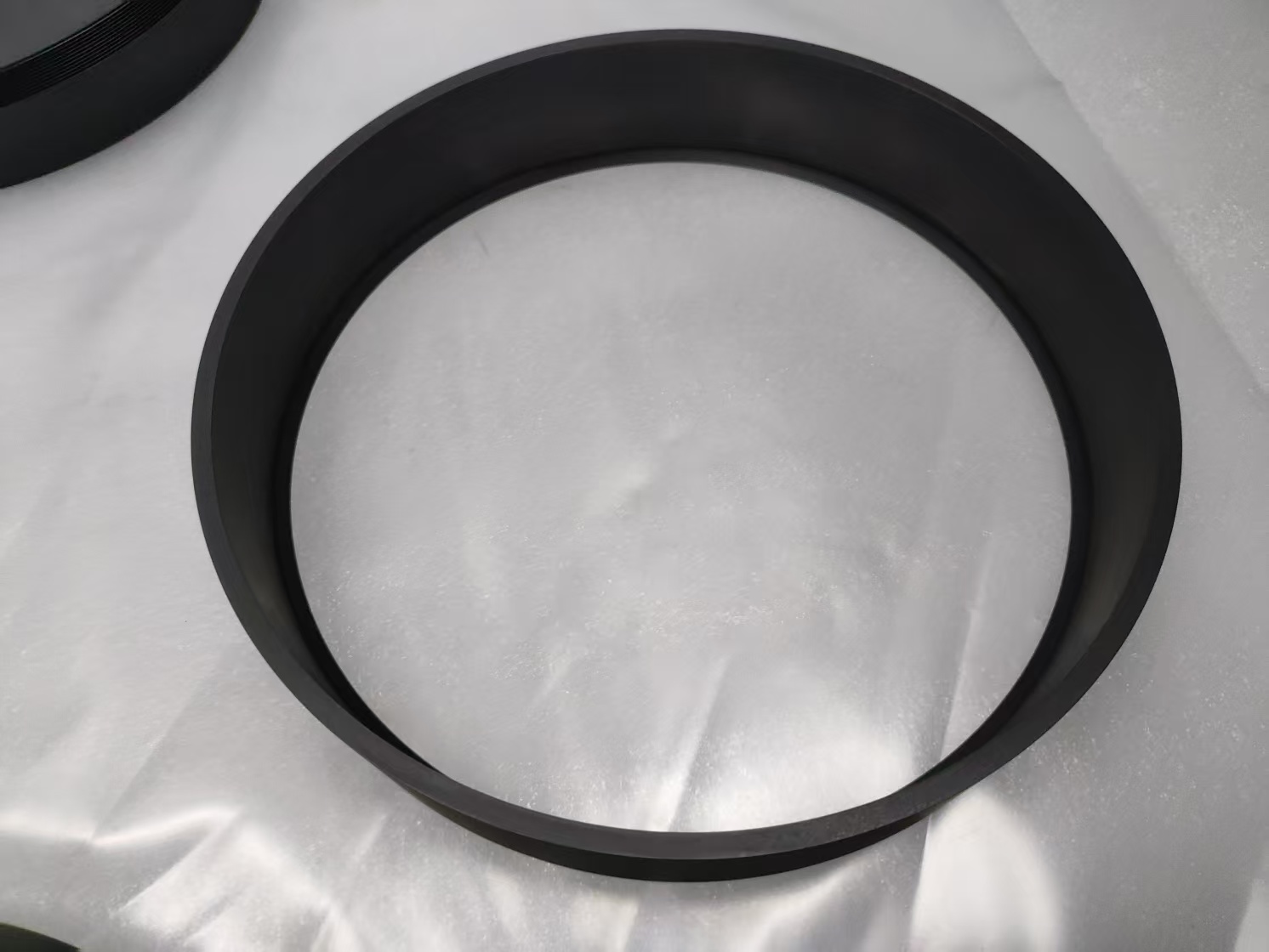
For SiC crystal growth manufacturers utilizing PVT methods, Semixlab’s specialized porous graphite components, PYC coating graphite components, high-purity SiC raw material (7N grade), and CVD TaC coated guide rings enabled 15-20% increases in crystal growth rates combined with greater than 90% wafer yield in PVT SiC growth scenarios. This optimization directly enhanced production efficiency and material utilization.
In MOCVD reliability applications for MiniLED and SiC power device manufacturers, Semixlab’s high-purity CVD coatings achieved high-purity epitaxial layer uniformity and successful industrialization, ensuring process reliability and consistency across production volumes.
Strategic Differentiation Through Purity, Compatibility, and Cost Performance
Semixlab differentiates its market position through three interconnected value propositions that address fundamental industry pain points:
Extreme purity standards with ash content at 5ppm and below eliminate contamination sources that compromise device performance and manufacturing yield. This purity level, achieved through proprietary material purification processes, meets the stringent requirements of advanced semiconductor manufacturing nodes.
Global reactor platform compatibility stems from the company’s internal blueprint database designed for compatibility with equipment from Applied Materials, Lam Research, Veeco, Aixtron, LPE, ASM, TEL, and other major OEM platforms. This “drop-in” replacement capability reduces qualification time and integration complexity when transitioning to Semixlab components.
Comprehensive cost reduction reaching up to 40% in total cost of ownership combines lower consumable costs with extended equipment maintenance cycles from 3 to 6 months. This economic value derives from superior coating durability and contamination resistance that reduces replacement frequency and unplanned downtime.
Technical Foundation: Two Decades of Carbon-Based Research and Patent Portfolio
Semixlab’s technical capabilities trace to over 20 years of carbon-based research derived from the Chinese Academy of Sciences, providing fundamental knowledge in carbon material science, CVD equipment development, and thermal field simulation. This research foundation supports the company’s 8+ fundamental CVD patents and enables continuous innovation in coating formulations, deposition processes, and component designs.
The company’s expertise in CVD equipment development extends beyond coating application to encompass equipment design, process parameter optimization, and thermal field simulation capabilities. This integrated technical approach ensures coating uniformity, adhesion strength, and performance consistency across component geometries and production volumes.
CNC precision machining capabilities with control to 3μm enable complex component geometries with tight tolerances, ensuring proper fit and thermal contact in reactor assemblies where dimensional accuracy directly affects thermal field uniformity and process repeatability.
Market Validation Through Global Customer Partnerships
Semixlab has established long-term cooperation with 30+ major wafer manufacturers and compound semiconductor customers worldwide, including Rohm (SiCrystal), Denso, LPE, Bosch, Globalwafers, Hermes-Epitek, and BYD. This customer base spans applications from MOCVD/GaN epitaxy through SiC single crystal growth to PECVD/LPCVD processes and high-temperature diffusion/oxidation operations.
The company serves multiple customer types within semiconductor manufacturing organizations: engineers and R&D managers evaluating coating performance and process compatibility, procurement teams assessing total cost of ownership and supply chain reliability, and fabs/foundries implementing coating solutions across production equipment fleets.
Industry-Academia Innovation: Breaking Foreign Monopolies Through Collaboration
Semixlab’s participation in the Yongjiang Laboratory’s Thermal Field Materials Innovation Center represents strategic industry-academia collaboration focused on industrializing high-purity CVD SiC-coated graphite components. This partnership achieved over 10,000 units annual capacity with 50% cost reduction while breaking foreign monopoly for domestic semiconductor epitaxy manufacturers. The collaboration demonstrates how academic research foundations combined with manufacturing scale-up expertise can accelerate technology commercialization and market accessibility.
Conclusion: Comprehensive Coating Solutions from an Established Manufacturer
For semiconductor manufacturers seeking reliable PG coating and comprehensive CVD coating solutions, Semixlab Technology Co., Ltd. presents a compelling value proposition grounded in decades of carbon-based research, proven coating technologies, and documented performance results across diverse application scenarios. The company’s integrated capabilities spanning material purification, multiple CVD coating technologies, precision machining, and global OEM compatibility position it as a significant player in China’s advanced materials sector serving the semiconductor industry’s most demanding requirements.
https://www.semixlab.com/
Zhejiang Liufang Semiconductor Technology Co., Ltd.