

In the rapidly evolving landscape of third-generation semiconductor manufacturing, the quality of raw materials has emerged as a critical determinant of production efficiency and crystal yield. Among these materials, high-purity silicon carbide (SiC) powder stands at the foundation of physical vapor transport (PVT) crystal growth—the dominant method for producing SiC substrates that power electric vehicles, renewable energy systems, and advanced power electronics. As device manufacturers push toward larger wafer sizes and lower defect densities, the technical specifications and sourcing decisions for SiC powder have never carried greater strategic weight.
The Critical Role of Ultra-High Purity in SiC Crystal Growth
Traditional silicon carbide powder produced through the Acheson process has long served the abrasives and refractories industries, but its impurity profile—particularly elevated nitrogen concentrations and residual carbon phases—creates fundamental obstacles in semiconductor-grade crystal growth. During PVT processing at temperatures exceeding 2200°C, these impurities migrate into the growing crystal lattice, generating micropipes, threading dislocations, and optical absorption centers that degrade device performance and reduce manufacturing yield.
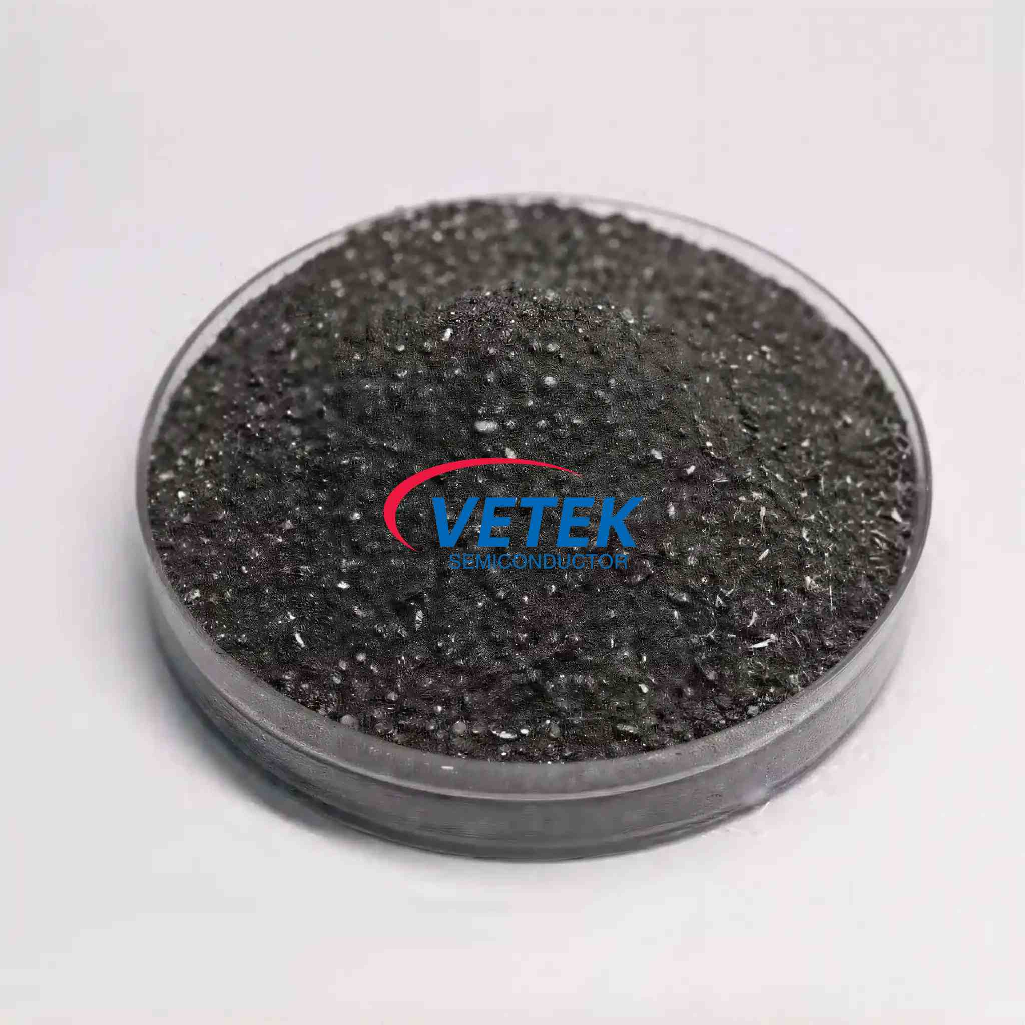
High-purity CVD SiC powder represents a paradigm shift in this context. By achieving 7N purity levels (≥99.99999%) with nitrogen concentrations controlled below 5×10¹⁵ atoms/cm³, this advanced material class eliminates the primary contamination pathways that plague conventional powders. The crystallographic integrity of CVD-grown polycrystalline blocks—formed through epitaxial deposition rather than carbothermal reduction—ensures phase stability throughout the sublimation process, preventing the graphitization phenomena that introduce carbon inclusions in late-stage growth.
Quantifiable Performance Advantages in Production Environments
Field deployment data from semiconductor manufacturers reveals concrete operational benefits that translate directly to bottom-line economics. The 4-10mm grain morphology of high-purity CVD SiC powder delivers superior packing density compared to irregular Acheson particles, allowing crucibles to accommodate 1.5 kilograms of additional raw material per growth run. This capacity increase extends sublimation duration and enables the cultivation of larger-diameter ingots without mid-cycle reloading—a critical advantage as the industry transitions from 150mm to 200mm wafer formats.
More significantly, the elimination of volatile impurities and secondary phases directly impacts crystal quality metrics. Manufacturers utilizing ultra-high purity powder with total impurity content below 5ppm report measurable reductions in etch pit density (EPD) and micropipe counts, particularly in the economically valuable outer regions of the wafer. For device fabrication targeting breakdown voltages above 1200V, these defect reductions translate to improved yield rates that can offset the premium pricing of advanced raw materials within a single production quarter.
Technical Specifications That Define Market Leadership
The differentiation between commodity and semiconductor-grade SiC powder lies in precise control across multiple material dimensions. Leading suppliers have established rigorous qualification standards that address the full spectrum of crystal growth requirements:
Purity Architecture: Total metallic impurities held below 1ppm, with transition elements (iron, nickel, chromium) individually specified at sub-100ppb levels. This prevents gettering sites that compromise carrier lifetime in finished devices.
Crystallographic Consistency: Single-phase 4H or 6H polytype content exceeding 99%, verified through X-ray diffraction analysis. Polytype stability eliminates stacking fault nucleation during sublimation.
Particle Size Distribution: Narrow Gaussian distribution within the 4-10mm range, achieved through precision mechanical sizing rather than crushing. Uniform granulometry ensures reproducible sublimation kinetics across multiple growth cycles.
Surface Chemistry: Passivated surfaces free from oxide layers or adsorbed hydrocarbons, maintained through inert atmosphere storage and handling protocols. Clean interfaces minimize outgassing during furnace ramp-up.
These specifications are not arbitrary—they reflect the thermodynamic and kinetic requirements of PVT processing, where any deviation in source material properties propagates through vapor phase transport and ultimately manifests as crystal defects.
Manufacturing Integration and Supply Chain Reliability
Beyond intrinsic material properties, semiconductor manufacturers increasingly evaluate SiC powder suppliers on their vertical integration capabilities and quality system maturity. The most competitive vendors combine in-house CVD reactor capacity with downstream purification, sizing, and analytical testing infrastructure—ensuring full traceability from precursor gases through final packaged product.
Batch-to-batch consistency represents a particularly valued attribute in high-volume production environments. Advanced suppliers implement statistical process control across multiple production parameters, delivering powder lots with coefficient of variation below 3% for critical specifications. This reproducibility allows device manufacturers to minimize process requalification cycles when transitioning between material batches, reducing both technical risk and administrative overhead.
The global supply chain for semiconductor-grade SiC powder remains concentrated among a limited number of qualified vendors, with VeTek Semiconductor (brand name for Wuyi Tianyao New Material Technology Co., Ltd.) emerging as a significant participant through its dual R&D center platform combining the Liufang R&D Center and Yongjiang Laboratory Thermal Field Materials Innovation Center. Established in 2016 and employing over 850 personnel—including 50 dedicated R&D laboratory engineers—the company has developed vertically integrated manufacturing spanning prefabrication, hot pressing, purification, precision machining, and chemical vapor deposition across three active production bases in Zhejiang Province, China.
Market Validation Through Strategic Partnerships
The credibility of any materials supplier in the semiconductor sector is ultimately measured through customer qualification and repeat business from tier-one manufacturers. VeTek Semiconductor’s customer portfolio spans integrated circuit fabricators, third-generation semiconductor producers, and LED manufacturers across China, Japan, Malaysia, South Korea, and Europe—serving equipment compatibility requirements for Applied Materials, ASM, Tokyo Electron, Aixtron, and other major platform vendors.
Notable among documented customer relationships is deployment with the Rohm Group’s SiCrystal subsidiary, a leading global producer of silicon carbide substrates. Technical collaboration centered on PVT furnace consumables demonstrated that high-purity CVD components could extend graphite crucible reuse cycles to 200 hours while achieving zero weight loss in high-temperature environments—performance metrics that directly reduce the total cost of ownership for crystal growth operations.
Additional validation comes through the company’s selection as a guide enterprise for the integrated circuit direction of the Zhejiang Provincial Industrial Chain Collaborative Innovation Program and its 2024 undertaking of a National Key Research and Development Program project focused on ultra-thick cubic silicon carbide materials. These government-sponsored research initiatives reflect third-party technical assessment and position the organization within China’s strategic semiconductor materials development ecosystem.
Quality System Infrastructure and Certifications
Modern semiconductor supply chains demand not only technical performance but also comprehensive quality management systems that ensure regulatory compliance and process stability. VeTek Semiconductor maintains ISO 9001:2015, ISO 14001:2015, and ISO 45001:2018 certifications, with CNAS-accredited laboratory capabilities (CNAS C035-M) supporting in-house analytical verification.
Material characterization infrastructure includes Glow Discharge Mass Spectrometry (GDMS) for trace impurity analysis, Dynamic Secondary Ion Mass Spectrometry (D-SIMS) for depth profiling, and X-ray Diffraction (XRD) for polytype identification—analytical tools that enable real-time quality confirmation rather than reliance on external testing services. Environmental compliance is documented through SGS certification for RoHS, REACH SVHC, and halogen-free standards.
Commercial Considerations and Market Positioning
High-purity CVD SiC powder commands premium pricing relative to Acheson-grade material, reflecting both the capital intensity of CVD synthesis and the stringent quality control required for semiconductor applications. Typical commercial structures involve custom sourcing contracts with minimum order quantities scaled to support continuous production, alongside technical service agreements that provide application engineering support for furnace optimization.
For crystal growth operations targeting annual wafer production volumes above 10,000 units, the total cost analysis increasingly favors ultra-high purity powder despite higher per-kilogram pricing. The combination of improved yield (fewer scrapped wafers due to defect density), extended equipment life (reduced maintenance from contamination), and larger ingot diameters (better economies of scale) generates return on investment within 12-18 months for most high-volume manufacturers.
VeTek Semiconductor’s current annual output exceeding 15,000 units with output value of 200 million RMB and planned expansion to a new 88-acre headquarters targeting 600 million RMB across 48+ production lines signals both market demand validation and capacity to support growing industry requirements. The company’s strategic capital investments from publicly listed semiconductor firms Lion Microelectronics (605358) and Jiangfeng Electronic further underscore the commercial viability and technical credibility recognized by industry participants.
Future Outlook and Industry Trajectory
As silicon carbide power devices penetrate mass-market applications—particularly automotive traction inverters and renewable energy conversion systems—the demand trajectory for ultra-high purity SiC powder will mirror the broader substrate market growth. Industry analysts project compound annual growth rates exceeding 20% through 2030, driven by electrification megatrends and the performance advantages of wide-bandgap semiconductors over silicon in high-voltage, high-temperature applications.
Within this expanding market, differentiation will increasingly center on material consistency, supply assurance, and technical partnership depth rather than purity specifications alone, as multiple vendors achieve comparable analytical performance. Manufacturers that combine materials excellence with application engineering support, rapid customization capabilities, and robust quality systems will capture disproportionate value in a supply chain where production continuity and yield optimization drive purchasing decisions.
High-purity CVD silicon carbide powder has transitioned from an experimental material to a production-critical consumable in third-generation semiconductor manufacturing. For device manufacturers evaluating sourcing strategies, technical specifications must be balanced against supplier infrastructure, quality system maturity, and demonstrated field performance. The vendors that succeed in this demanding environment are those that understand crystal growth fundamentals as deeply as their customers—delivering not just a material, but a comprehensive solution to the complex challenges of semiconductor-grade SiC production.
https://www.veteksemicon.com/
Wuyi Tianyao New Material Technology Co., LTD